AMD’s $10 Billion Bet on Taiwan’s AI Future
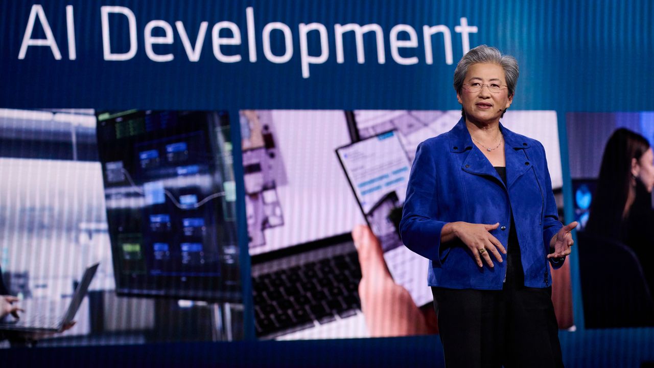
The race to dominate next-generation AI infrastructure is heating up, and AMD is making a massive move to secure its place at the top. In a significant strategic shift, the company announced today that it is investing more than $10 billion into the Taiwan semiconductor ecosystem. This substantial capital injection is designed to scale advanced packaging facilities and expand critical partnerships, ensuring AMD remains at the forefront of the AI revolution.
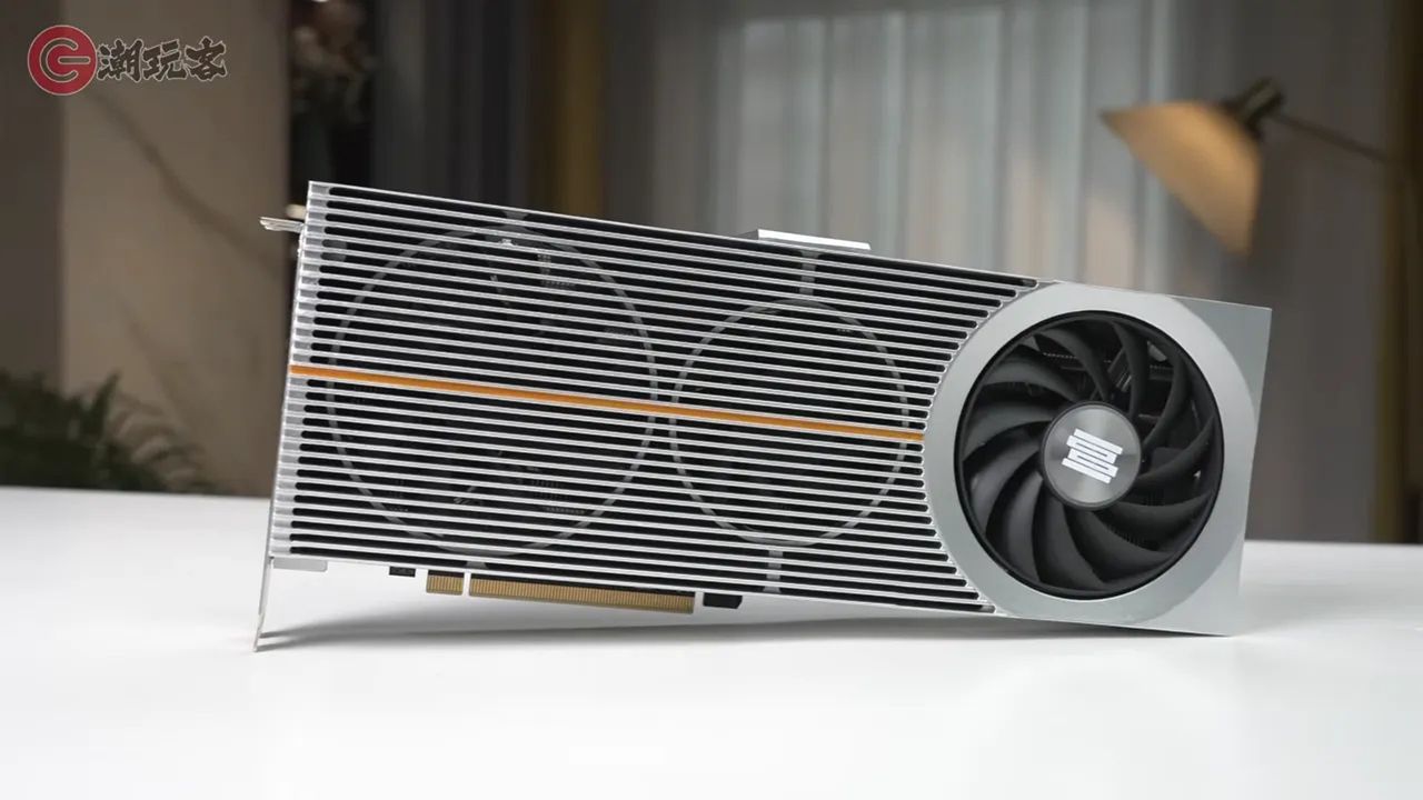
This isn't just about spending money; it's about building the physical backbone for the future of computing. AMD aims to accelerate the deployment of its most powerful hardware yet, including the upcoming Helios rack-scale platform, by strengthening its ties with key partners like ASE and Silicon Precision Industries.
Scaling Advanced Packaging for Real-World Constraints
A significant portion of this investment is earmarked for the development of next-generation interconnect technology. Specifically, AMD is focusing on wafer-based, 2.5D bridge tech to support its upcoming Venice CPUs. This technical leap is crucial for improving chip power efficiency, addressing one of the biggest hurdles in AI data center design: heat and energy consumption.
The industry has long been plagued by unrealistic expectations regarding cooling and power. AMD’s new approach is explicitly designed to create efficient AI systems that operate within "real-world power and cooling constraints," rather than the fantasy scenarios often cited in theoretical data center planning.
Key technical goals of this initiative include:
- Developing 2.5D bridge technology to enhance connectivity between chip components.
- Improving overall power efficiency to support multi-gigawatt AI workloads.
- Supporting the deployment of the Helios rack-scale platform in the second half of this year.
- Integrating Instinct MI450X GPUs with 6th Gen EPYC CPUs for seamless performance.
Venice Epyc and the Road to 2nm
Beyond packaging, AMD and TSMC have announced a major production milestone: the ramping up of Venice Epyc CPUs on TSMC’s cutting-edge 2nm technology in Taiwan. This marks a critical step in the transition to next-generation silicon, promising significant performance gains over previous generations.
While Taiwan remains the primary hub for these advanced processes, AMD is also looking toward its domestic capabilities. The company confirmed future plans to ramp up production at TSMC’s Arizona fab, diversifying its manufacturing footprint while maintaining high-volume output for its enterprise customers.
"This investment across Taiwan’s ecosystem will help us scale advanced packaging and accelerate next-gen AI infrastructure, from 6th Gen EPYC CPUs codenamed 'Venice' to our Helios rack-scale platform," AMD stated in its announcement.
A Strategic Move for a $720 Billion Giant
For a company with a market cap exceeding $720 billion, a $10 billion investment is a substantial commitment. However, in the high-stakes world of AI hardware, the margins for error are slim. By combining silicon innovation with a robust global ecosystem, AMD is positioning itself to enable customers to deploy AI systems faster and more efficiently than ever before.
As the demand for AI processing power continues to skyrocket, AMD’s focus on advanced packaging and real-world efficiency sets it apart from competitors still wrestling with theoretical limitations. With Venice Epyc CPUs coming online and the Helios platform on the horizon, AMD is clearly preparing for the next era of artificial intelligence.