While I wouldn’t claim to be a data center expert—PC gaming circuitry is much more my bread and butter—it is impossible to ignore the "RAMpocalypse" currently underway. Everyone seems to know that these massive servers are stacking memory like nobody's watching. This is why OpenAI's hilarious new patent diagrams have become such a viral sensation, sparking waves of bewilderment across social media.
Breaking the JEDEC Standard
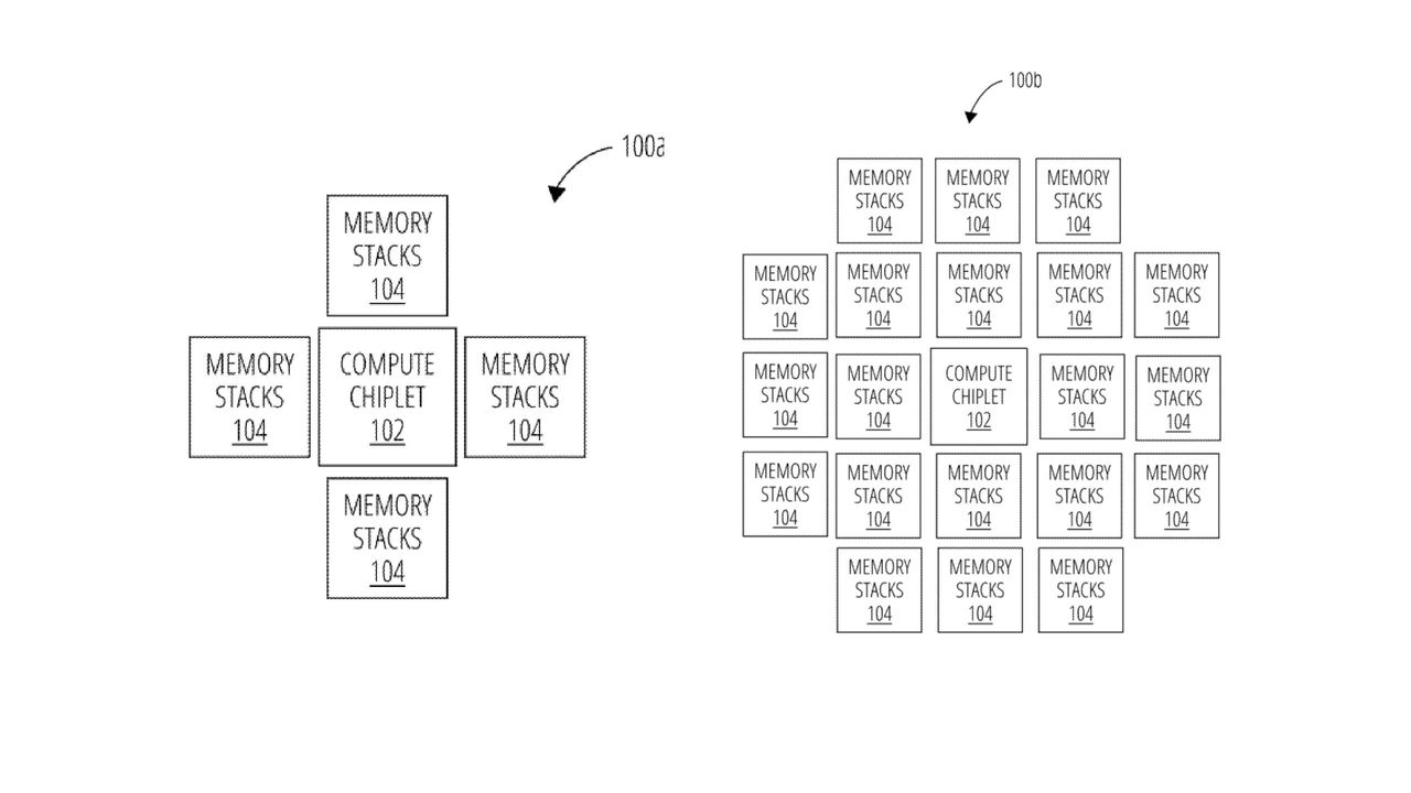
The chip architecture patent, published on April 2, 2026, outlines a specific system designed to push the boundaries of memory capacity. The filing describes a system of high bandwidth memory (HBM) chiplets and compute chiplets that utilize specialized components to expand performance.
According to the patent, the design includes:
- Embedded logic bridges used to facilitate communication.
- Extended communication distances between chiplets.
- A way to bypass the ~6 mm limit imposed by the JEDEC standard.
The technical goal is to allow HBM chiplets to communicate with other chiplets far beyond traditional distance constraints.
Social Media Reacts to OpenAI's Hilarious New Patent Diagrams
The reaction to OpenAI's hilarious new patent diagrams has been nothing short of chaotic. On X, users have been sharing the incredibly simple diagrams that show a massive amount of memory crammed alongside a single compute chiplet. It essentially screams, "You've heard of memory, but have you heard of more memory?"
The internet's commentary highlights the sheer scale of the hardware being proposed:
- One patent analyst noted that the HBM is "stacked up like rice cakes."
- Citrini research analyst Jukan asked, "What the hell is this thing?" while suggesting Sam Altman ("Sama") is trying to buy up all available memory.
- Korean users also chimed in, joking about the "HBM plastered everywhere" approach and expressing a mix of amusement and hope for the technology's success.
Putting a patent on the concept of essentially adding "more memory" might seem wild, though I admit that is a simplification. There are undoubtedly complex technical hurdles involved in getting those HBM stacks to communicate effectively across such distances from the central compute chiplet.
While there are more specific diagrams in the filing to examine, the sheer audacity of the design is hard to miss. If these companies are determined to continue gobbling up our precious DRAM, we at least deserve a laugh at their expense.