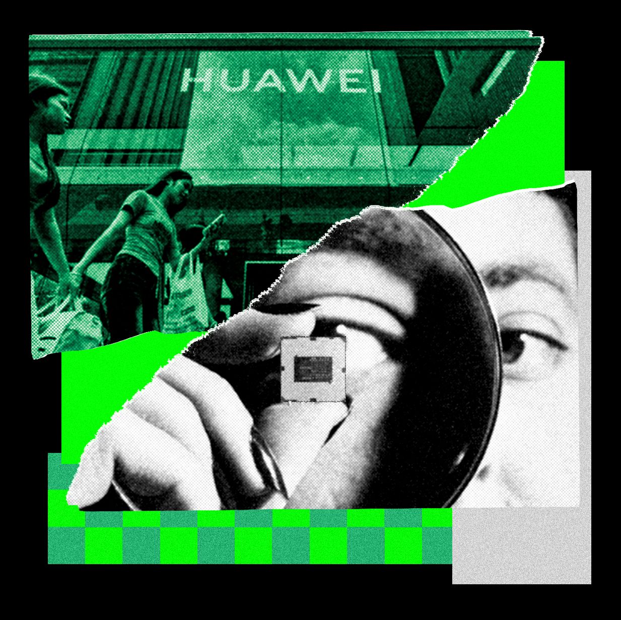
A decade after being severed from global semiconductor supply chains, Huawei has not only survived but surpassed its rivals by building a complete chip ecosystem from scratch. This paradox defines the current era of Chinese tech: while American policymakers viewed the company as a telecommunications vendor destined to be strangled by sanctions, its semiconductor division quietly evolved into a fully integrated powerhouse capable of challenging the world's most advanced foundries. At the center of this transformation is Huawei’s ‘Chip Queen’, a leadership figure whose relentless drive for vertical integration has turned isolation into an unexpected competitive advantage.
The Rise of Huawei’s ‘Chip Queen’ Under Sanctions
Under the guidance of prominent chip architect He Tingbo, Huawei has cultivated a comprehensive portfolio spanning system-on-chip design, optoelectronics, and advanced packaging. Rather than outsourcing core components, the tech giant developed deep capabilities across the entire hardware stack. This vertical integration allows engineers to optimize performance directly at the silicon level while bypassing traditional manufacturing bottlenecks through innovative chiplet architectures.
The narrative surrounding this leadership blends technical acumen with strategic vision, positioning Huawei as the last bastion of Chinese semiconductor self-reliance. By reducing reliance on external suppliers for everything from RF front-ends to baseband processors, the company has built a defensive moat that competitors find difficult to breach. He Tingbo’s influence is particularly evident in the dual focus on general-purpose computing and artificial intelligence, ensuring the hardware supports diverse workloads ranging from consumer devices to massive cloud infrastructure.
Advanced Packaging Meets System-Level Optimization
U.S. sanctions beginning in 2019 cut Huawei off from key foreign chip technologies and leading-edge manufacturing, threatening its core businesses with irrelevance. Instead of folding, the company pivoted toward advanced packaging and heterogeneous integration to bridge the gap left by restrictive export controls. This approach treats physical packaging as a performance multiplier, stacking memory and logic layers to boost bandwidth without waiting for the next generation of lithography tools.
The strategy reveals a commitment to reaching cutting-edge performance through architectural ingenuity rather than relying solely on photolithography improvements. By prioritizing software-hardware co-design, Huawei challenges the industry consensus that shrinking transistors is the only path to higher efficiency. This architectural shift cements the legacy of Huawei’s ‘Chip Queen,’ who recognized early that bottlenecks could be solved at the system level rather than through raw transistor density alone.
Throwing Down the Silicon Gauntlet
The company is no longer merely surviving sanctions. By reshaping the global semiconductor landscape from the inside out, Huawei has thrown down a definitive gauntlet for the rest of the industry to follow. This strategic pivot ensures that domestic innovation will continue to dictate global hardware trends for years to come.
The foundation of this resurgence rests on four key pillars:
- Kunpeng processors delivering competitive server performance for enterprise data centers
- Ascend AI accelerators dominating domestic machine learning workloads with high-throughput inference capabilities
- Custom optical interconnects reducing latency and power consumption in high-bandwidth applications
- Proprietary EDA tools accelerating design iteration cycles while minimizing dependency on foreign software
As domestic foundries scale up production and global export restrictions continue to tighten, maintaining innovation velocity requires sustained investment in both design and manufacturing equipment. Huawei has proven it can architect world-class silicon; the next phase demands that this momentum translate into mass-market dominance across consumer and enterprise segments.